
Teaching Assistant Project: Construction of RISC-V SoC and HDMI Peripheral on FPGA
This project is a teaching practice and hardware upgrade initiative supervised by Professor Huang Jiye at Hangzhou Dianzi University. Originally planned to be carried out by graduate students assigned by the instructor, the task was independently undertaken and completed by me during my junior year while serving as a teaching assistant for the course "Digital Systems and Processor Laboratory" (In the theoretical component of this course, I ranked 2nd out of 55 students with a GPA of 4.6/5; I achieved a perfect GPA in the laboratory component, and was thus selected by the instructor.), while guiding sophomore students in mastering the use of Quartus tools and the fundamentals of Verilog HDL design.Abstract
This project upgrades the Cyclone10LP FPGA development board used in the digital electronics laboratory course, replacing the original VGA display interface in the SoC systemwith a more versatile and widely adopted HDMI peripheral interface,successfully completing hardware adaptation and logic development, and achieving iterative optimization of the experimental platform's peripheral functions. To accomplish this comprehensive task, the validity of the 720P@60Hz video link on the FPGA was first verified, resulting in two engineering demos: a color bar display and an HDMI music score player. Based on the verified RTL functionality, an HDMI display peripheral was integrated into the RV32I SoC system. Reliable solutions were provided for cross-clock-domain data interaction (CDC issues) between the CPU system clock domain and the pixel clock domain, as well as for timing/pixel alignment issues caused by display pipeline latency. Finally, a digital clock demo programmed in C for the SoC was used for verification. The results demonstrated that the HDMI peripheral on the SoC could stably output 720p signals, with clear character display free of glitches and capable of continuous refresh, thereby completing the project.
Objectives of the Teaching Assistant Task
Task 1 Completed: Driver and Teaching Engineering Migration
Implemented the FPGA HDMI driver and produced a color bar demo; on this basis, migrated the original VGA image engineering to HDMI, verifying the usability of complex applications.
Task 2: SoC HDMI Peripheral Integration
Integrate HDMI character display into a five-stage pipelined RV32I SoC, forming an MMIO access model where the CPU writes to video memory for display, and complete a digital clock demo for verification.
FPGA HDMI driver implementation
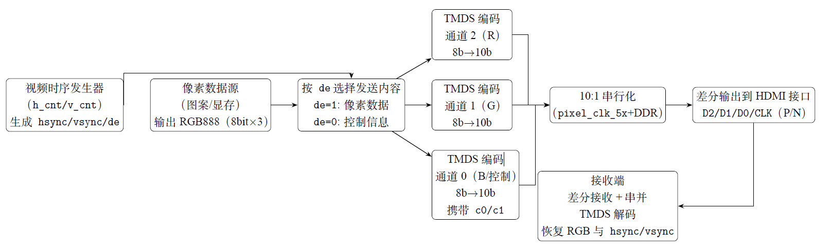
First, regarding the hardware implementation of FPGA HDMI, this project only uses the DVI-compatible "video transmission" part, which is characterized by not sending images in packet form, but by scanning and outputting in rows and frames as a continuous pixel stream. The transmitter is responsible for generating video timing, and the receiver samples and restores the RGB data of each pixel at the correct time points based on the timing.In the transmission process, HDMI adopts TMDS encodingto reduce signal transitions and achieve DC balance. This includes encoding each 8-bit pixel information, horizontal/vertical synchronization signals, and the active display enable signal into TMDS, and implementing the encoding using an IP core. At the receiver end, the display performs serial-to-parallel conversion and TMDS decoding under the differential CLK signal, thereby continuously recovering the per-pixel RGB data stream. The following figure summarizes the HDMI video stream encoding and output process as summarized by the author:
Required Signal Transmission Lines for HDMI (Hardware Pinout)
| Signal Name | FPGA Pin | Signal Name | FPGA Pin |
|---|---|---|---|
HDMIB_D2_P | B8 | HDMIB_D0_P | F15 |
HDMIB_D2_N | A8 | HDMIB_D0_N | F16 |
HDMIB_D1_P | B9 | HDMIB_CLK_N | G16 |
HDMIB_D1_N | A9 | HDMIB_CLK_P | G15 |
The above table corresponds to 3 pairs of TMDS data differential pairs (D2/D1/D0) and 1 pair of clock differential pairs (CLK), totaling 4 differential line pairs.
| Parameter | Horizontal (H) | Vertical (V) | Description |
|---|---|---|---|
| Sync Pulse | 40 | 5 | H_SYNC / V_SYNC |
| Back Porch | 220 | 20 | H_BACK / V_BACK |
| Active Display | 1280 | 720 | H_DISP / V_DISP |
| Foreword | 110 | 5 | H_FRONT / V_FRONT |
| Total | 1650 | 750 | H_TOTAL / V_TOTAL |
HDMI music score player
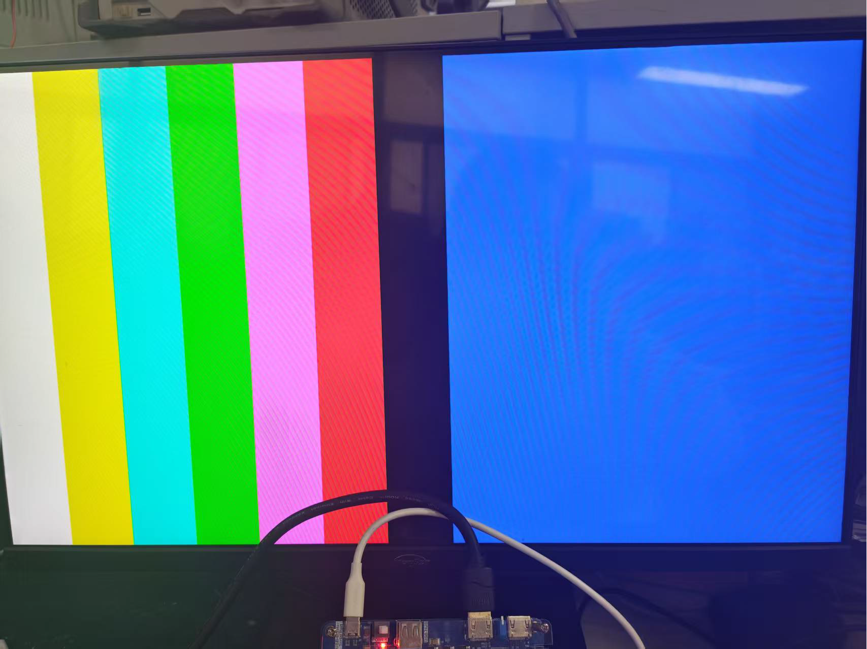
Based on the above fundamental principles, combined with the open-source FPGA-HDMI RTL available online, it is possible to constructa top-level HDMI-Display application module.By specifying the row and column pixels of the application module, a complete color bar display can be obtained. Similarly, for the HDMI music score player, additional modules for music score image display, border drawing, and dynamic box overlay are designed to achieve HDMI display of the music score image and indication of the current note position. The HDMI display effects are as follows:
SoC HDMI Modification and CDC Issues
After the full implementation of the HDMI hardware, the video peripheral modification of the SoC begins. First, a basic understanding of this SoC is required. This is an open-source teaching SoC from USTC, written in SystemVerilog,featuring an RV32I CPU (excluding CSR instructions) as its core, adopting a Princeton architecture. It can be used as an MCUand includes peripherals such as UART, instruction ROM/RAM, data RAM, video RAM with VGA output, and LEDs/digital tubes. The corresponding assembly/C language compilation tools have been configured and open-sourced (see the project repository: https://github.com/WangXuan95/USTC-RVSoC) (this is an upgraded version by the author). The CPU employs a classic five-stage pipeline (IF: instruction fetch, ID: instruction decode, EX: execution, MEM: memory access, WB: write-back). The bus does not conform to any existing standard; it is a simple synchronous handshake bus. The bus arbiter is connected to three master interfaces (CPU data and instruction fetch, UART debugging) and six slave interfaces (all of which can be extended or modified). Each slave interface occupies a specific address space. When a master interface accesses the bus, the arbiter determines which address space the target address belongs to through hardware computation based on the target address and the starting address of each slave interface, and then routes the access to the corresponding slave interface.
| Slave Device | Address Range | Function |
|---|---|---|
| Slave0 | 0x0000_0000 – 0x0000_0FFF | Instruction ROM |
| Slave1 | 0x0000_8000 – 0x0000_8FFF | Instruction RAM |
| Slave2 | 0x0001_0000 – 0x0001_0FFF | Data RAM |
| Slave3 | 0x0002_0000 – 0x0002_0FFF | VideoRAM(HDMI) |
| Slave4 | 0x0003_0000 – 0x0003_0003 | User UART |
| Slave5 | 0x0003_1000 – 0x0003_100F | LED / SEG |
Note:Slave3 A 4KB address window is reserved at the bus layer.0x0002_0000~0x0002_0FFF), 64×8 character grid basis, and the actual access is to the first 512B video memory region.
After gaining a basic understanding of the SoC principles in this project, the focus is onanalyzing the original VGA peripheral, including the VideoRAM and the VGA character display module. Character display primarily follows these steps: timing generation, locating the character to be displayed, requesting the ASCII code to be displayed, querying the 8×16 dot matrix font, and outputting pixels.The VideoRAM consists of four M9K blocks on the FPGA. After the CPU fetches instructions, it writes ASCII codes to the bus, while the VGA display module continuously reads the video memory for display. Meanwhile, the font information is stored in the VideoRAM.
After understanding the original VGA display principle, the HDMI peripheral was ported.Essentially, this involves solving the CDC (Clock Domain Crossing) problem at the hardware interface of the driver layer—namely, how to achieve safe and reliable cross-clock-domain data transmission between the CPU operating in the 50MHz system clock domain and the HDMI 720P@60Hz display logic operating in the 74.25MHz pixel clock domain, while ensuring precise alignment of timing signals and pixel data under a 6-stage pipeline delay. This is the main challenge of the entire project.In contrast, the VGA display driver is much simpler, as it does not involve CDC issues and can operate entirely within the 50MHz clock domain along with the CPU and bus. Traditional CDC solutions include double flip-flop synchronization chains (for single-bit signals), handshake protocols (for multi-bit data but requiring complex request-acknowledge logic), and asynchronous FIFOs (requiring additional read/write pointer management and empty/full detection). However, these solutions are either unsuitable for 512-byte large-capacity storage or significantly increase design complexity and latency.
The inapplicability of traditional FIFO solutions to this CDC problem
The semantics of a traditional FIFO do not match the video memory model of this project.In this system, the CPU side performs
addr/byte_en random address updates on character units, while the display side performs sequential scanning and reading of the current frame state based on pixel timing. The HDMI display reading involves periodically re-reading hdmi_ram the set display content. This is not a unidirectional data flow where the write order equals the read order and data consumption is balanced.
The continuous throughput requirement of the display link determines that a FIFO is not a suitable carrier for this task.In 720p mode, the HDMI pixel path must continuously supply data at a rate of
74.25MHz sustained throughput. Once a FIFO becomes empty or full, it directly results in screen artifacts, tearing, or discontinuous output. Moreover, data read from a FIFO is consumed immediately and is not suitable for preserving the persistent state of "current screen content."
If a FIFO were to be used, system complexity would not decrease.The project would either need to retransmit the entire screen data every frame or still require a RAM in the HDMI clock domain to maintain repeatable reading within a frame. Additionally, the visibility of CPU writes would require extra confirmation or barrier mechanisms. Considering semantic matching, timing stability, and implementation cost, this project does not adopt a "pure FIFO" as the core CDC solution.
Solving the CDC problem with dual RAM mirroring and parallel writes
To completely avoid the CDC problem while maintaining design simplicity and enabling the rapid implementation of this educational project, I adopted a "space-for-time" dual-IP-core dual-port RAM solution. The core idea is to first eliminate the conflict of different clock domains reading and writing the same device. Therefore, two completely independent 512-byte video memory RAM copies are prepared for the CPU and HDMI, respectively. The CPU-side RAM operates in the 50MHz clock domain, while the HDMI-side RAM operates in the 74.25MHz clock domain.The write ports of both RAMs are connected to the bus; therefore, when the CPU executes a Store instruction to write characters into the video memory, the write enable signal wren simultaneously activates both RAMs (single IP_RAM2P Essentially, this is a Simple Dual Port (single write, single read)), causing the same data to be written to the same address of both RAMs at the same moment (based on a 50 MHz clock),thereby achieving the effect of replicating the HDMI RAM. In terms of read operations, the CPU reads data from the CPU-side RAM through its own read port (this is a purely same-clock-domain read operation, with no latency or risk), while the HDMI display module reads data from the HDMI-side RAM through its own read port (this is also a same-clock-domain read operation, as the read port clock of the HDMI-side RAM is connected to the 74.25 MHz pixel clock). The two read operations proceed independently within their respective clock domains, with no intersection whatsoever, thus completely eliminating the CDC (Clock Domain Crossing) issue. The dual-port RAM IP core provided by Altera has already handled the scenario where the write port and read port use different clocks (through dedicated multi-clock-domain SRAM macro cells and built-in synchronization circuits). Therefore, designers do not need to manually write any cross-clock-domain logic; they only need to correctly configure the IP core parameters. The cost of the dual-RAM scheme is a doubling of hardware resources, but stability is fully guaranteed, and design complexity is significantly reduced. Thus, the upgrade of the HDMI peripheral on the SoC is completed.
For the HDMI peripheral of this SoC, the VideoRAM can be designed as "write-only, no read." In that case, the HDMI mirror in the CPU clock domain can indeed be removed. Alternatively, a software shadow VRAM scheme can be adopted in the C/assembly language compilation for SoC users, automatically copying the content written to VideoRAM into DataRAM, thereby achieving both readability and writability. However, the software dual-write approach increases the number of instructions and bus pressure, resulting in poorer real-time performance. Additionally, it requires constraints at the hardware or compilation level to treat a portion of DataRAM as VideoRAM that cannot be arbitrarily written to—such a design is overly complex and difficult to stabilize. For digital hardware system design, directly using hardware to achieve a stable solution at the ISA-invisible layer is a better design outcome.
Student approach to using the SoC HDMI with C language
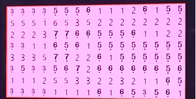
From the student's perspective, there is no need to understand these relatively complex architectural principles. Instead, they only need to use the C language to define ASCII characters for specified address spaces.This is because the well-designed hardware ensures stable execution of ISA instructions. After programming the SoC, the HDMI immediately displays characters at the corresponding positions, and character transitions can be controlled through software delays. Through teaching practice, multiple second-year students have successfully developed other applications, such as PWM character flashing displays, based on this HDMI-SoC platform, verifying the system's ease of use and stability. The display effect of the HDMI-SoC clock demo characters is shown in the figure below:Student-side C language code snippet: Writing characters to VideoRAM
#define VRAM_BASE 0x00020000

                void putchar_at(int row, int col, char c) {
                    volatile unsigned char *vram = (unsigned char *)VRAM_BASE;
                    int addr = row * 64 + col;
                    vram[addr] = c;
                }

                int main() {
                    int hour = 12, min = 0, sec = 0;
                    while (1) {
                        putchar_at(3, 0, '0' + hour/10);
                        putchar_at(3, 1, '0' + hour%10);
                        putchar_at(3, 2, ':');
                        putchar_at(3, 3, '0' + min/10);
                        putchar_at(3, 4, '0' + min%10);
                        putchar_at(3, 5, ':');
                        putchar_at(3, 6, '0' + sec/10);
                        putchar_at(3, 7, '0' + sec%10);
                        delay_1s();
                    }
                }
Summary
This teaching assistant project has completed the full closed loop from "driver availability" to "system availability":
Open-source code repository address
ChrisChan114514/HX1006B-MOOC-Lab
FPGA HDMI Experiment Project Open-Source Repository
ChrisChan114514/SocHDMI
RV32I SoC HDMI Peripheral Upgrade Open-Source Repository
PDF Report
If the browser cannot preview PDF directly, use the "Open in New Window" button.