
Digital Systems and Processors Course and Its Laboratory Implementation
"Digital Systems and Processors" is one of the core courses in the Honors College Experimental Class. In this course, I achieved high scores in both theoretical and laboratory components. Based on the fundamental VGA experiment, I also developed an interactive digital clock system, transforming the experimental requirement of "pre-configured driver layer with independent application-layer development" into a complete FPGA engineering implementation.
Course Background and Performance Overview
The course ran from September 2024 to January 2025. *Digital Systems and Processors* was offered to two sophomore experimental classes in Electronic Engineering and Integrated Circuits, instructed by Professor Huang Jiye The course covers digital logic, RTL design, 74LS series circuit applications, and fundamentals of DAC/ADC.
Academic Performance
Theory course: 91 points (GPA 4.6/5, ranked 2nd out of 55)
Laboratory course score: 99 (GPA 5.0/5, course record 95)
Subsequent extensions
Based on my performance in this stage, I was selected by the instructor as a teaching assistant for the Digital Electronics Laboratory course in my junior year, and further undertook teaching projects related to RV32I.
Characteristics of laboratory training
The VGA experiment adopted a "driver-layer preset, application-layer independent development" approach, focusing on assessing the ability to extend functionality based on existing low-level timing.
Experiment Overview
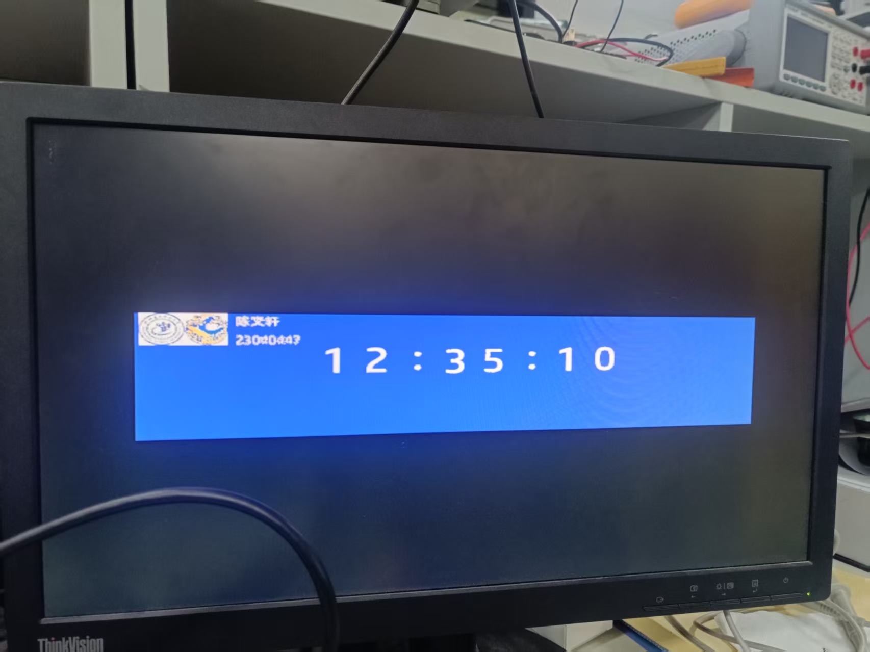
This experiment was based on the Altera Cyclone 10 LP FPGA, upgrading the basic VGA display experiment into a functioning digital clock display system.
Final implemented functions
Real-time on-screen display HH:MM:SSButtons for fast time adjustment; digits and colons are stably output via ROM pixel lookup table.
Development Process and Steps
Part 1: Understanding the main role of the application layer
Provided code vga_disp Outputs current pixel coordinates at 25MHz x/y And display window control; the application layer receives these contexts at each clock cycle.
Part 2: Application-layer time state update
I defined rom_rgb.v In total_seconds As the global time state, updated once per second, and injected different stepping strategies based on key[1:0]
Step 3: Decompose the global time and perform display mapping
Let total_seconds Decompose into hours、minutes、seconds, then through region encoding {y[6:5], x[8:5]} determine which digit or colon the current pixel belongs to.
Step 4: Semantic Mapping to Pixels
The digit semantics are first mapped to background indices (ZERO..NINE/MAOHAO), and then walk.mem + walk_pal.mem output 12 bits via a lookup table rgb。
Step 5: Driver Layer Completes Physical Output
The driver layer is only responsible for timing and gating: output in the active region rgb, clear the non-display area, and HSYNC / VSYNC ensure stable locking of the display.
key + clk25M + x/y → total_seconds → digits → background_id → rgb → VGA_D
Understanding the VGA Driver Layer
1. VGA Standard Clock Domain
pll.v Divide the 50MHz clock down to 25MHz to match the standard pixel clock of VGA 640×480.
2. Horizontal and Vertical Scanning
vga_disp.v Use hcnt / vcnt Dual counters implement progressive horizontal and vertical scanning to form a complete frame timing sequence.
3. Synchronization Signals
Pull low within the specified counting window HSYNC / VSYNCto declare the horizontal and vertical synchronization boundaries to the display.
4. Active Display Gating
First, map the 512×128 content area to the center of the 640×480 display, then dis_en Output RGB in the effective display region, and set the non-display region to zero.
5. Frame-Level Update
vs_flag It can serve as a frame edge signal, supporting subsequent logic such as character/animation updates at frame synchronization points.
6. RGB Data Path
The application layer determines x/y output 12-bit rgb, and the driver layer sends it to the effective display region VGA_D, forming the final screen pixels.
Key Code Snippets
vga_disp.v: Effective Display Region and Synchronization Signal Generation
assign x = (hcnt >= (640-512)/2) ? hcnt-(640-512)/2 : 11'h7ff;
assign y = (vcnt >= (480-128)/2) ? vcnt-(480-128)/2 : 11'h7ff;
assign dis_en = (x<512 && y<128);

if((hcnt >=640+8+8) & (hcnt < 640+8+8+96))
  hs <= 1'b0;

if((vcnt >= 480+8+2) && (vcnt < 480+8+2+2))
vs <= 1'b0;rom_rgb.v: Button-Controlled Time Stepping and Digital Display
if (time_counter == 25000000) beginvga_cartoon.qsf: Board-Level Pin Constraints (Excerpt)
set_location_assignment PIN_P16 -to VGA_HSYNC
set_location_assignment PIN_N15 -to VGA_VSYNC
set_location_assignment PIN_E15 -to clk50M
set_location_assignment PIN_M1  -to reset_n
set_location_assignment PIN_E1  -to key[1]
set_location_assignment PIN_F3  -to key[0]
Project Preview and Files
Key Project Files (View Original Source)
Notes and Repository Preview
Note Preview (Final Summary)
Organized key points of the Digital Electronics course, experimental debugging records, and the final review framework to facilitate quick review and reflection.
GitHub Project Preview
ChrisChan114514/HDU-digital-electricity-experiment-open-source
Open-source Lab Course Code GitHub Repository (18 Stars)